
PCB Fabrication
These are my notes on how to get a PCB designed in KiCAD fabricated by OSH Park. The process is easy- there isn’t anything complex or tricky. I just like to have a reference to follow.
These notes were developed while ordering the TLPHnodeV2
Design Rules
The first step is to make sure that the PCB matches the OSH Park Design Rules. The best way is to configure KiCAD with the appropriate rules before you start to layout the board.
The TLPHnodeV2 is designed as a 4-layer board, so the rules are:
* 5 mil trace clearance
* 5 mil trace width
* 10 mil drill size
* 4 mil annular ring
The rules are entered in the Pcbnew->Design Rules->Design Rules dialog.
A good trick is to set the board units to inches
(Pcbnew->Preferences->General) to enter the values even if you are going
design your board using metric values. After you have entered the
minimums, you can set the board units to mm and Pcbnew will
automatically translate the entered values to the new units.
The other trick is that Pcbnew expects Minimum via diameter, but OSH Park provides only the annual ring value. To get the minimum diameter, add 2x the annular ring to the minimum drill size.
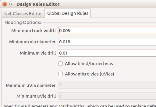
Before attempting to submit a design to OSH Park, make sure you run the Pcbnew Design Rule Checker.
Preparing the design
While OSH Park will accept KiCAD files directly, I like to plot gerber files from KiCAD and check them manually so that I know exactly what I am sending to OSH Park.
OSH Park provides clear instructions for KiCAD two-layer boards. Four-layer boards are not much different.
Plot
For a four layer board these layers should be selected:
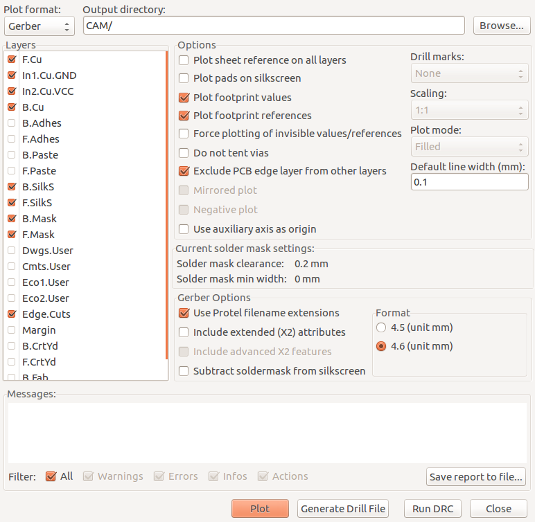
Note that while OSH Park says that they accept KiCAD output names, but only a 2-layer board was detected for the TLPHnodeV2- probably because I changed the names of the inner layers.
To get OSH Park to recognize all four layers I had to select Use Protel
filename extensions.
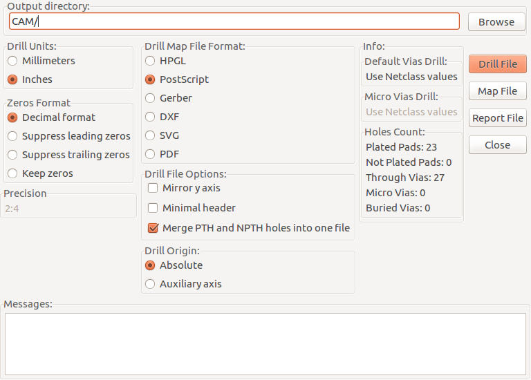
Drill File
The drill file settings are the same as the ones in the OSH Park
instructions. The only changes I had to make from the
KiCAD default were to un-check the Minimal header and select the
Decimal Format.
Verify
I use gerbv to view the files. For a 4-layer board, there should be 10 files.
    $ cd CAM/
    $ gerbv *.g* *.drl
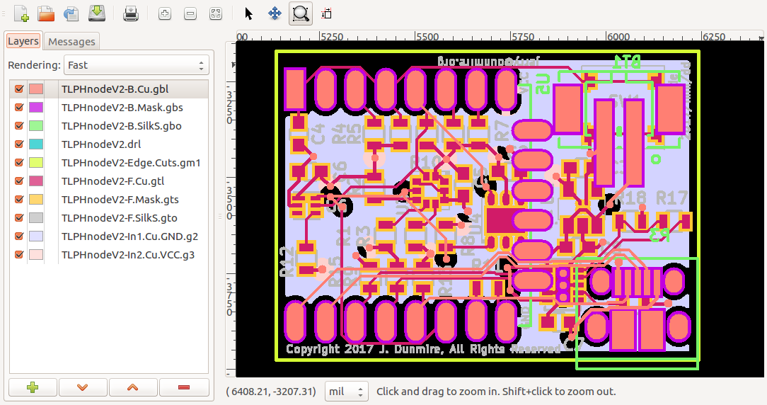
I look to make sure that the holes and masks line up. I look for traces that exposed because they pass through an open mask area. Such traces can produce shorts during soldering:

I also look to make sure that the silk-screen markings don’t cover any pads.
Upload
OSH Park expects all of the gerbers and the drill file to be combined into one zip file:
    $ cd CAM/
    $ zip <project>.zip *.g* *.drl
The project upload starts on the OSH Park Home page. Once the file has been uploaded and processed the Processing Upload page will be displayed:
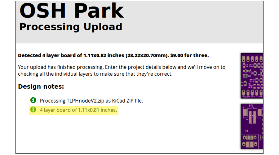
Make sure that a 4-layer board was detected and that the size is about what you expect.
Subscribe
Subscribe to this blog via RSS.
Categories
Firmware 1
Hardware 5
Console 1
Tools 4
Recent Posts
-
 Posted on 16 Jan 2017
-
 Posted on 12 Jan 2017
-
Posted on 24 Jan 2016
-
Posted on 19 Jan 2016
Popular Tags
Background (2) Firmware (1) Hardware (5) Infrastructure (1) Console (1) T&l node firmware (1) Tools (4) Tlphnodev2 (2)

